Stratophase relocated to a new facility in Romsey, UK, on 14 July 2010. The new facility is much larger than the old one, and is expected to double the sensor manufacturing capacity of Stratophase.
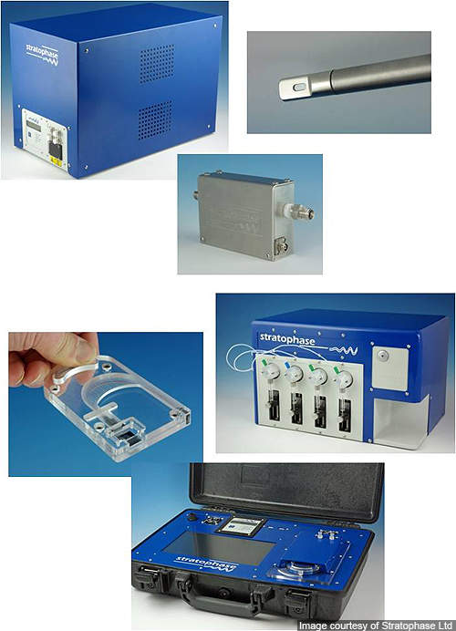
It will allow Stratophase to quickly respond to a range of application requirements by improving the facilities where new techniques for optical measurement are implemented, and tested on Stratophase sensor chips as well as the systems that use these chips.
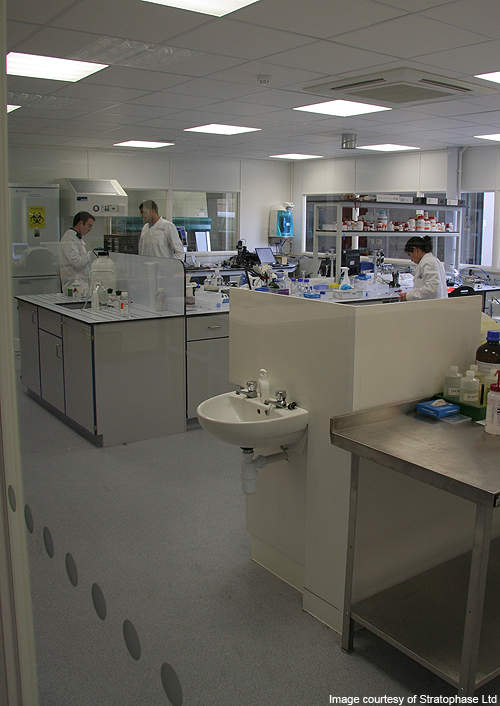
Stratophase’s Romsey laboratory
The new facility is three times the size of the old facility. It includes space for administration, meetings and state-of-the-art laboratories. It also has space for future expansion that can be undertaken without causing much disturbance.
The laboratories accommodate an exclusive Category 2 biological containment laboratory and a customer applications laboratory. The high-tech laboratories allow the company to functionalise immunoassays on sensor chips for the purpose of biodetection and test the monitoring systems for use in industrial processes such as biorefining and biofuels production, pharmaceuticals and fine chemicals.
Production
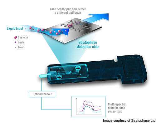
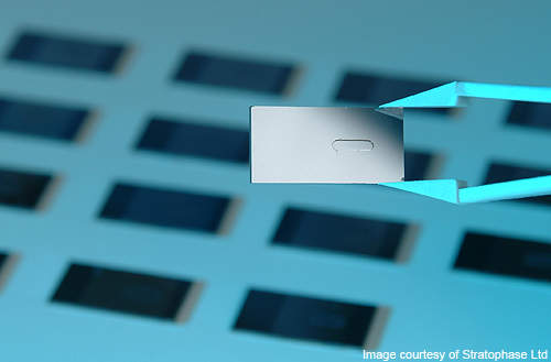
The new facility will develop optical microchip sensors with high-precision planar Bragg gratings. These sensor chips that generally measure up to a few tens of square millimetres are used to monitor the fermentation process in bio-production. It is capable of measuring chemical processes and at the same time detects all types of biological targets including proteins, bacteria and viruses on the same microchip.
The sensing surface of the chip is carefully bonded with antibodies in a manner that allows simultaneous sensitivity to several targets.
When the target antigen attaches to the antibodies on the sensing surface the refractive index alters, changing the wavelength of light reflected from the Bragg gratings.
The rapid detection of toxins and pathogenic micro-organisms offers an instant response against a host of target antigens, avoiding the need for sampling and laboratory testing.
Technology
The optical microchips will be developed using Stratophase’s proprietary direct writing technology. This technology inscribes waveguide structures including couplers, splitters and Bragg gratings onto glass layers. The combination of gratings and waveguide is inscribed over a three layered planar silica-on-silicon substrate that is deposited using flame hydrolysis deposition. The central layer that forms the core is germanium-doped to provide photosensitivity to radiation at 244nm.
The remaining two layers are also co-doped with other elements in a way that results in identical refractive index for all three layers. To further improve the photosensitivity, the sample is stored for three days in hydrogen at 150bar. During this process, hydrogen in-diffusion into the silica core takes place.
The direct grating writing technology uses a continuous Ar+ laser to define the waveguide as well the gratings at the same time. Using this technology, several Bragg gratings and waveguides can be placed anywhere within a single chip. The waveguides are placed in a cross-sectional dimension similar to fibre cores, while the sensors measure between one millimetre to tens of millimetres in length.
Once the waveguide is defined, the overclad layer on top of the grating section of the chip is removed using a wet etch process. Hydrofluoric acid in a timed etch removes the clad (which usually measures ~1% of the chip’s thickness) without damaging the waveguide core.
To collect liquid water on top of the sensor, an approximately 0.5mm-thick aluminium window is attached to the sensor’s surface as side walls.
The device is fibre pigtailed to facilitate constant in and out coupling of light.
The direct grating writing technology can measure variances in refractive index as small as 10–6.
It also provides temperature compensation benefits, measuring temperature differences up to 0.01°C for refractive index sensing.

